原理图
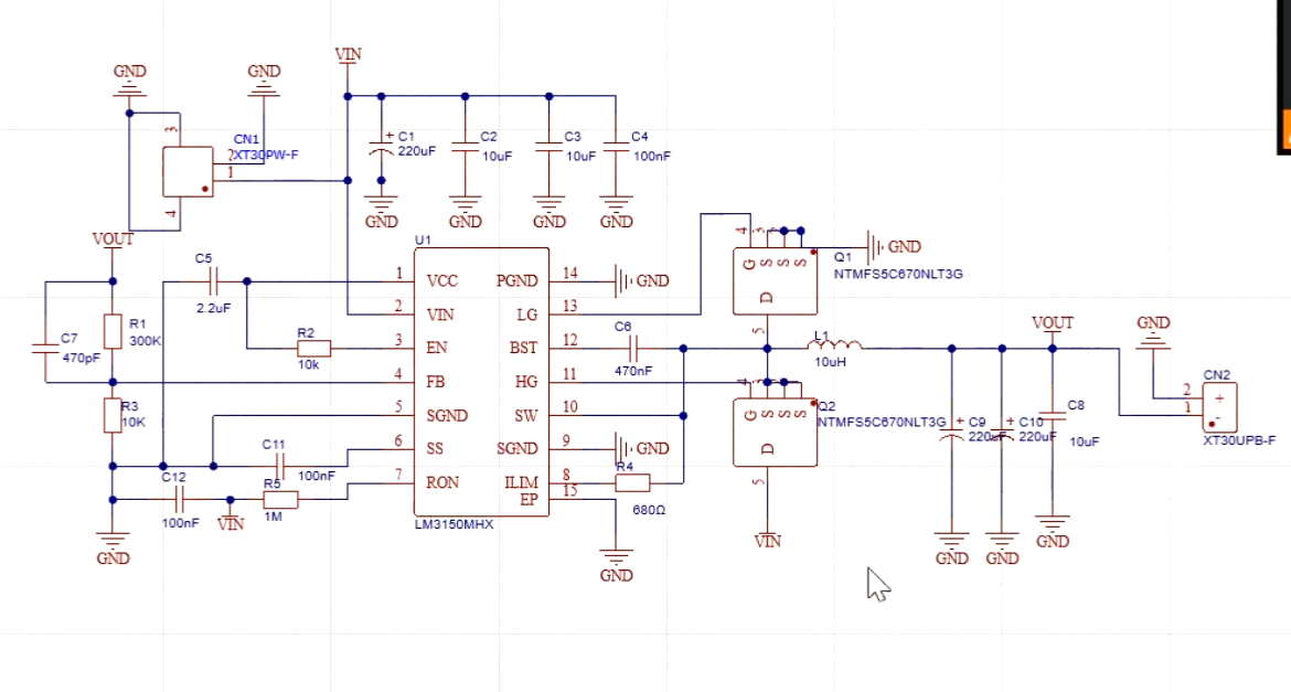
芯片引脚分析
VCC
Nominally regulated to 5.95V. Connect a 1.0 µF to 2.2 µF decoupling capacitor from this pin to ground.
Design Guide要求串联一个容值在1.0uF和2.2uF的电容,可以看到图中C5是一个2.2uF的电容串联接地。
VIN
Supply pin to the device. Nominal input range is 6V to 42V.
明显此脚接电源输入,电压范围在6V到42V。
EN
To enable the IC apply a logic high signal to this pin greater than 1.26V typical or leave floating. To disable the part, ground the EN pin.
引脚需要给一个高于1.26V的输入电压来让芯片工作,或者电压保持浮动,原理图上选择串联一个10k电阻。Electrical Characteristic里给出的电压范围是1.14V~1.26V。
没找到应该怎么算这个电阻的阻值(还是说整个值仿真一下之后发现行就怼上去了),Design Guide还要求其工作在开漏状态时应串联一个1000pF的电容(推荐值)。
FB(FeedBack)
Internally connected to the regulation, over-voltage, and short-circuit comparators. The regulation setting is 0.6V at this pin. Connect to feedback resistor divider between the output and ground to set the output voltage.
似乎此脚的输入电压应该调到0.6V,并且连接到输出和接地之间的反馈电阻用以调整输出电压。
SGND
Ground for all internal bias and reference circuitry. Should be connected to PGND at a single point.
信号地,应该和PGND连一起。
SS(Soft Start)
An internal 7.7 µA current source charges an external capacitor to provide the soft-start function.
此处需外接一电容,充电后提供软起动功能
计算公式
$$
C_{SS}=\frac{I_{SS}t_{SS}}{V_{ref}}
$$
其中$V_{ref}=0.6V$,$I_{SS}=7.7 \mu A$,$t_{SS}$需要在开始的几秒之内测出来?(我理解是这个意思)
RON
Function:An external resistor from VIN to this pin sets the high-side switch on-time.
从VIN到该引脚的外部电阻设置高压侧开关接通时间。
由datasheet有以下关系
$$
D=\frac{t_{on}}{t_{on}t_{off}}=t_{on}f_s \approx \frac{V_{OUT}}{V_{IN}}
$$
易得
$$
f_s=\frac{V_{OUT}}{K R_{on}}
$$
其中K为常数,$K=100pC$。
PGND
SGND里写了
ILIM(Current Limit)
Monitors current through the low-side switch and triggers current limit operation if the inductor valley current exceeds a user defined value that is set by $R_{LIM}$ and the Sense current, $I_{LIM-TH}$, sourced out of this pin during operation.
监控通过低压侧开关的电流,如果电感器谷电流(最小电流)超过用户定义的值(由$R_{LIM}$设置),则触发电流限制操作,并且在操作过程中检测电流$I_{LIN-TH}$来自此引脚。
由datasheet,$R_{LIM}$可以按下方算式进行估计
$$
\begin{equation}\begin{split}
&I_{CL}=I_{OCL}-\frac{\Delta I_L}{2} \
&R_{ILM}=\frac{I_{CL}R_{DS(on){max}}}{I{LIM-TH}}
\end{split}\end{equation}
$$
其中$I_{OCL}$是自定义的最大输出电流,$R_{DS(on){max}}$是低位MOS管在预期最大MOS管温度下的电阻值,$I{LIM-TH}$典型内部电流源为$85 \mu A$。
还有一个
$$
\Delta I_L=\frac{(V_{IN}-V_{OUT})t_{on}}{L}
$$
SW(Switch Node)
Switch pin of controller and high-gate driver lower supply rail. A boost capacitor is also connected between this pin and BST pin
SW和BST之间连接一个升压电容
Design Guide推荐值为0.47uF
此外SW向外连接了一个电感(续流?),直接输出VOUT
这里不是很懂,但是Design Example上是这样的。
HG(High-Side Gate Drive)
Gate drive signal to the high-side NMOS switch. The high-side gate driver voltage is supplied by the differential voltage between the BST pin and SW pin.
高位NMOS的Gate信号端,Design Example上面上下两个MOS管连在了一起,上位的D连接下位的S。(为啥..?)
BST(Connection for Bootstrap Capacitor)
见SW
LG
Gate drive signal to the low-side NMOS switch. The low-side gate driver voltage is supplied by VCC.
低位NMOS的Gate信号端,VCC直接给低位NMOS供电。
PGND
Synchronous rectifier MOSFET source connection. Tie to power ground plane. Should be tied to SGND at a single point.
和SGND连一起。
电压输入与输出附近
注意到在$VIN$和$VOUT$的附近都有三四个电容,放电容的意义是起一定的缓冲作用,相当于微型UPS用以保护芯片。我怎么觉得不止这一个作用
输出和输入端用了两个连接器(XT30PW-F和XT30UPB-F),用以连接供电线缆
电压输出大小
根据Design Guide有
$$
V_{OUT}=V_{FB}\frac{R_{FB1}+R_{FB2}}{R_{FB1}}
$$
其中,$R_{FB1}$是下方的电阻,$R_{FB2}$是上方的电阻,
上方原理图中,$R_{FB1}$为10k,$R_{FB2}$为300k,$V_{FB}$为0.6V
经计算得
$$
V_{OUT}=18.6V
$$